
An Introduction To Power Factor — How To Control It In Your Med Device Design
By Jeff Prsha, Design Engineer, A2e Technologies

Why do we use alternating current (AC) power? Why don’t power companies just distribute direct current (DC) power, since the first thing we normally do with modern appliances is convert the AC to DC? The answer to those questions dates back to Thomas Edison’s efforts to promote his incandescent lamp and electrify New York.
Edison’s generators produced DC power, which worked fine for local distribution, but required either very large cables to supply loads more than a few blocks away, or a power station every few blocks. This is because, at voltages practical for end use, large currents were required to electrify more than just a small area. Enter Nikola Tesla, backed by George Westinghouse, who promoted high-voltage AC transmission lines with a low voltage substation every few blocks for local distribution. The important difference was the substation only required a transformer, while the DC solution required a complete steam-powered power plant.
Ultimately, Westinghouse settled the war that ensued when he built a hydroelectric plant at Niagra Falls that was able to supply loads hundreds of miles away. However, in the few extremely long, point-to-point transmission lines, the balance tips back toward very high voltage DC transmission lines (e.g., the power line from Grand Coulee Dam in Washington State to Los Angeles).
AC power enabled many other inventions key to industrialization, from the induction motor and gas discharge lamp ballasts to light dimmers and electric shavers. But part of the dark side of AC power is this notion of power factor. The voltage for DC power is constant, so there is no phase associated with it; AC power is (ideally) sinusoidal, with the voltage and current crossing 0 V at 120 times a second (twice per 60 Hz cycle). If the load (or even the power line) is slightly inductive or capacitive, the current will either lag or lead the voltage.
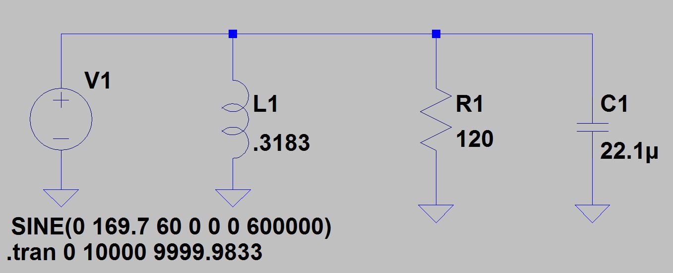
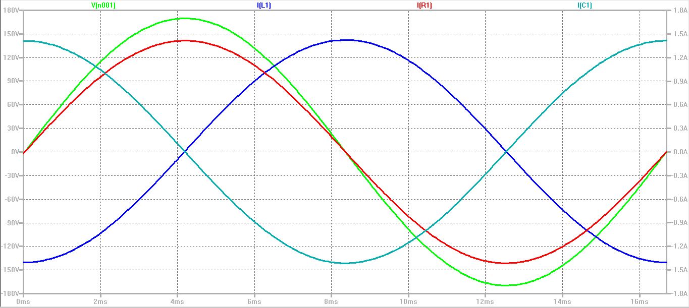
Figure 1 shows an LTspice model of a 120 VAC, 60 Hz, AC voltage source driving an inductor, a resistor, and a capacitor in parallel. Figure 2 shows the output of this simulation with the voltage of the source V(n001), the inductor current I(L1), the resistor current I(R1), and the capacitor current I(C1). Notice that only the resistor current is in phase with the voltage, the inductor current “lags” behind the voltage by 90 degrees, while the capacitor current “leads” the voltage by 90 degrees.
How (And Why) To Determine Power Factor
Power factor is classically defined as the cosine of the angle between the root mean square (RMS) AC voltage — defined as the amount of AC power that produces the same heating effect as DC power — and the RMS AC current. To calculate the power consumed by a DC load, simply multiply the voltage at the load by the current through it. To calculate the power consumed by an AC load, the product of RMS voltage and current must be multiplied by the power factor.
If voltage and current are in phase (0 degrees phase error), the cosine of 0 is 1, and therefore the same calculation as DC. This occurs when the load is made to look resistive. If the phase error is 60 degrees, the cosine of 60 is 0.5; only half of the product of voltage and current is delivered to the load. So where does the other half go? That current still circulates through the power lines; it just doesn’t deliver useful power to the load.
When breaking down the “apparent power” waveform (called volt-amperes, or VA) into its in-phase and out-of-phase parts — sometimes referred to as “real” and “imaginary” parts, respectively —the in-phase part (the cosine coefficient) is called power (measured in watts), while the out-of-phase part (the sine coefficient) is called reactive power (measured volt-amps-reactive, or VAR). So, power factor can also be defined as the real power divided by VA (PF = W/VA). The watt meter on your power panel only measures real power, so customers are only billed for real power, but the utility still has to size its equipment to handle the total current flowing, so it strives to make all current “billable” current.
But why does any of this matter, particularly if you are not billed for it? First, the utility ultimately bills its customers for all expenses, so the cost of correcting power factor is passed on to consumers. Second, more and more agency specifications — such as EN60601, EN61000, and IEC555 — require power factor correction for medical devices (sometimes referred to as powerline harmonic control). Manufacturers of medical devices are required to provide varying degrees of power factor correction in their products, depending on power output and application. If you are thinking, “My product does not contain any large loads, much less inductive or capacitive types,” there is a subtlety that rears its ugly head: That little switching power supply you put into your product to meet the efficiency/wide input/size/weight/packaging requirements introduces its own peculiar variant of power factor corruption.
Remember, a power factor of one occurs when the load appears resistive. A switch mode power supply (SMPS) typically rectifies the power line, and then charges a large capacitor to store energy during the time the voltage sine wave drops to 0V, until it recovers. If this capacitor is large enough, it will store enough energy that the power line can drop out or “brown out” for several cycles, such as occurs when a large load is connected to the line (e.g., air conditioning compressors starting or laser printer heaters cycling). From a power supply designer’s point of view, the bigger that input capacitor, the better. If the capacitor is big enough, it discharges very little during a cycle of the power line, and during steady state, the power line voltage is only greater than the capacitor voltage at the positive and negative peak of the waveform. Therefore, current only flows during the peaks of the power line voltage waveform.
It is perfectly in phase, so the power factor should be 1, right? Well, remember that the load should appear resistive. Figure 4 shows the AC current waveform of a resistive load and that of a switching power supply at equivalent power levels. Notice that the resistor produces the expected in-phase sinusoidal waveform, while the switcher front end produces an impulse of current twice per cycle. A pulse is the superposition of multiple sine waves, since this pulse occurs at regular intervals, the sine waves that make up the pulse must all be harmonically related. In this case, 60Hz is the fundamental and the other sine waves are harmonics of 60Hz.
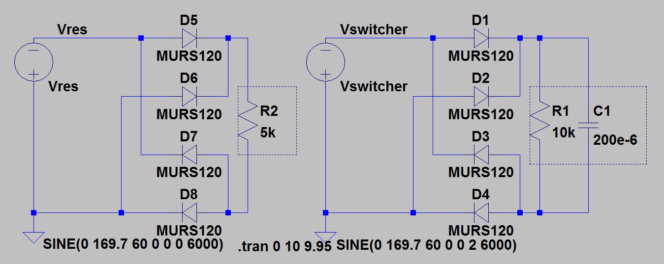
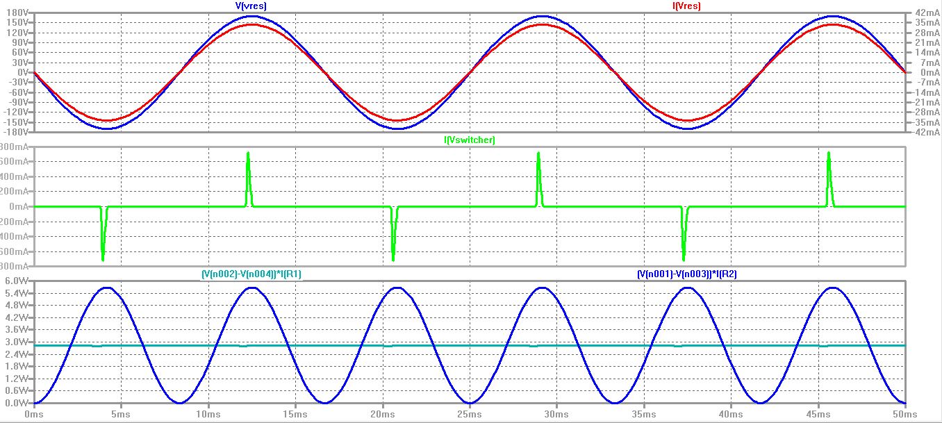
The topology of the front end of a simple, offline, switching power supply is illustrated on the right side of Figure 3. The AC voltage source (Vswitcher) is rectified by the four diodes and charges a capacitor (C1). Normally, the switching power supply would operate from the energy stored on the capacitor (the power dissipated by R1 simulates a load on the supply). For comparison, the left half of Figure 3 shows the waveform with just a resistive load (R2). Figure 4 illustrates the waveforms of these circuits. As expected, the voltage and current are in-phase for the resistive load shown in the top pane. There will be a small discontinuity close to the zero crossing due to the diode forward voltage, but that is not visible here because of the scale.
The applied voltage is the same for the switcher front end, but the resultant current is shown in the middle pane. Notice the scale of the current (shown on the right side of the top pane) is about 20 times greater in the middle pane (800 mA peak vs 40 mA peak). The bottom pane shows that both circuits consume the same power, measured by the voltage across the resistor multiplied by the current through it. R1 is larger than R2 because R1 is operating at approximately 169 VAC, while R2 is operating at 120 V RMS, but the power dissipated in each is the same. This illustration is something of a worst case, but it shows how much higher peak currents can be for a switched mode input than a resistive load operating at the same power level.
Harmonic Generation And Three-Phase Power Generation
Two consequences result from the switcher input current waveform in power lines where a large number of switching supplies are installed. First, because a large pulse of current is required at the peak of the line, instead of spreading this over the whole cycle, the voltage sags due to resistive drop in conductors and saturation in transformers or uninterruptable power supplies. This distorts the voltage waveform and generates further powerline harmonics. Even though the current pulse is timed with the peak of the voltage waveform, only the fundamental frequency is truly in phase with the voltage; the harmonic currents flow in and out of the capacitor while the diode is “on,” but do not store significant charge in it. The RMS ammeter measures all of the harmonic current, but the real power is just the energy stored in capacitor each cycle. Therefore, the product of the RMS current and voltage will show an indicated apparent power greater than the real power.
Distributed throughout IEC 60601 are paragraphs reclassifying medical devices that would otherwise pass International Special Committee on Radio Interference (CISPR) requirements, except for their distortion of the third harmonic of the powerline. This applies particularly to devices with loads greater than 75 W and less than 16 A per phase. Third harmonic distortion can be generated by any non-linearities in the load, but most commonly derive from switched mode power supply (SMPS) front ends.
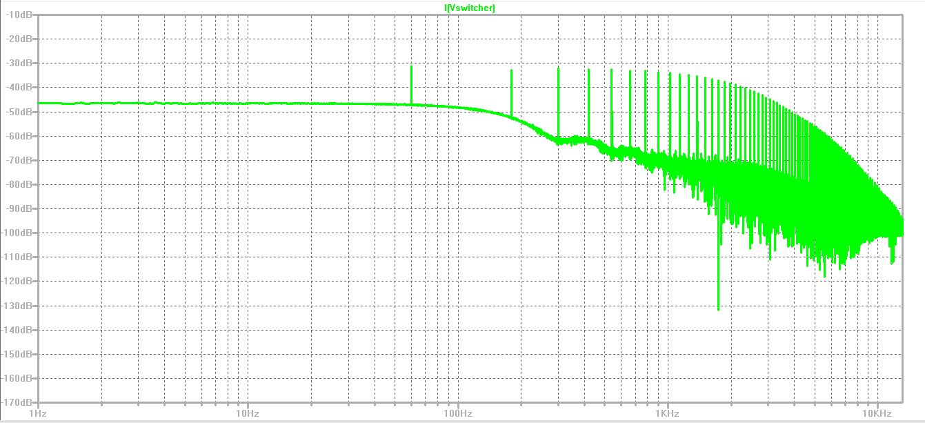
Figure 5 is a spectral analysis (performed by FFT) of the current in the middle pane of Figure 4 (the simulated input current to a SMPS). Amplitude is shown on the y axis and frequency is shown on the x axis (both axes are plotted on a logarithmic scale). A purely sinusoidal input current would have a single peak at 60 Hz, but the distorted waveform of Figure 4 shows the fundamental at 60 Hz, plus an almost equally large spike at 180 Hz (third harmonic of 60), accompanied by a plethora of higher harmonics.
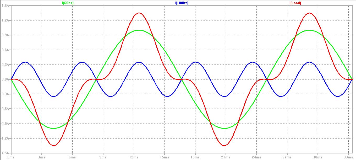
To see the effect of just the third harmonic targeted by 60601, Figure 6 shows the superposition of a 60 Hz current [green trace labeled I(60Hz) with its third harmonic I(180Hz)]. The resultant waveform I(load) shows what looks similar to the input current of a SMPS. Notice that the current is disproportionately low on either side of the zero crossing and then peaks with the voltage. The characteristic waveform of the SMPS input current is specifically addressed by 60601.
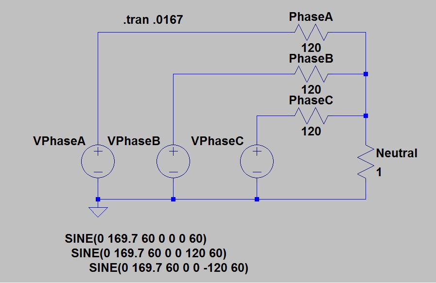
Beyond this harmonic generation, a second consequence (of switcher input current waveform in power lines where a large number of switching supplies are installed) is the phenomenon of three-phase power generation. This is easiest to understand in “WYE” (Y) configuration where three phases, 120 degrees apart, all share a common neutral, as shown in Figure 7.
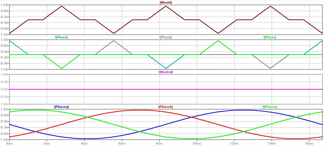
Imagine a resistive load connected from each phase: A, B, and C, to the neutral wire. Without descending into the math, imagine phase A is at the peak of its positive excursion, phase B will be delayed 120 degrees, and phase C will be delayed 240 degrees (which is the same as leading phase A by 120 degrees). The current flowing into resistor R1 is exactly equal to the sum of the current flowing out of R2 and R3. The bottom pane of Figure 7 shows the three currents flowing in each of the three phase resistors. The current in that neutral wire is zero as long as the load is perfectly balanced. The neutral current, I(Neutral) is shown at approximately 0 in the second pane from the bottom.
This is true for any chosen phase angle: The current in all three phases will balance. In fact, the neutral wire is only there to deal with minor imbalances between the phases, and it typically is the same gauge wire as each phase wire. Now, replace sinusoidal drive in the three phases with a triangular pulse, similar to the switching power supply examined above. The overlay of the three triangular phase waveforms is shown in the second pane from the top of Figure 8. Now, when phase A is at the peak of its positive excursion and it generates that big current spike, the other two phases are not carrying any current, and the neutral must carry all of the return current. Since the neutral is the same size as the phase wire, what’s the problem? Well, rotate the phase 120 degrees and phase B will hit its peak and supply the same current which the neutral will need to carry, then rotate the phase until phase C hits its peak. In one cycle of the power line, the neutral had to carry three times the current of each of the phase wires. This is the current shown as I(Neutral) in the top pane. Even in the best outcome scenario, the neutral wire gets very hot and the voltage sags considerably more than expected.
Controlling Power Factor In Your Device
OK, so controlling power factor may be something to be concerned about; what can be done to fix it? The good news is that semiconductor companies are working hard to sell you a solution. If your design is close to meeting your requirements without power factor correction, revisit that design and look at the input voltage range your switching IC will operate down to (or choose a new one) with lower input limit. Reduce the size of that input capacitor to increase the input conduction angle and spread that current spike over time (more like a resistor). Of course, doing this will make your supply more susceptible to drop out and brown out. Increasing the size of the output capacitors will help some, but this starts to take up quite a bit of space and can introduce other problems. Passive 60 Hz bandpass filters for the power line also are available, but they tend to require considerable space, as well.
Alternatively, you can add a power factor corrector (PFC) to your design. Some switching controllers incorporate power factor correction, but independent front ends are most common. The simplest independent front end to understand is a “constant on-time” (COT) boost converter. It is inserted between the power line and that input capacitor, which caused all the problems above. This PFC has practically no input capacitance (other than the X and Y capacitors in the filter) and, as the name implies, it uses a constant on-time boost topology to charge that input energy-storage capacitor to a voltage greater than the highest peak of the power line the device is designed to see.
For example, if the high line was 120 VAC + 10 percent (120 X √2 X 1.10 = 187 V), 200 V may be chosen as the boost voltage. The boost controller would turn on the boost inductor for a period of time brief enough to prevent it from saturating at the peak of the line. A “fast” control loop drives the inductor switching, so that each switch cycle is “on” for the same period. Since the inductor current equals LVt (L = inductance, V = voltage, and t = time) — with L and t held fixed — inductor (I) current and therefore power line current are proportional to V. Since I is proportional to V, the input looks resistive.
This might work acceptably for a fixed power level, but if the load fluctuates, the output voltage will vary wildly. To solve this, the boost controller actually has two loops: The fast loop described above, and the slow loop, which adjusts the “on” time to control the capacitor voltage, but does so slowly, over several power line cycles, to keep that resistive appearance. The capacitor voltage is only loosely regulated, which means that the capacitor has to be sized and rated to accommodate the variation. But, because the boost circuit makes the input to the capacitor appear resistive, the capacitor can now be relatively large. Because this topology is a boost converter, if the output (energy storage capacitor) voltage is ever less that the input voltage, current will flow from input to output to charge the capacitor. In this case, the power supply would continue to operate just fine, but the power factor correction would be defeated.
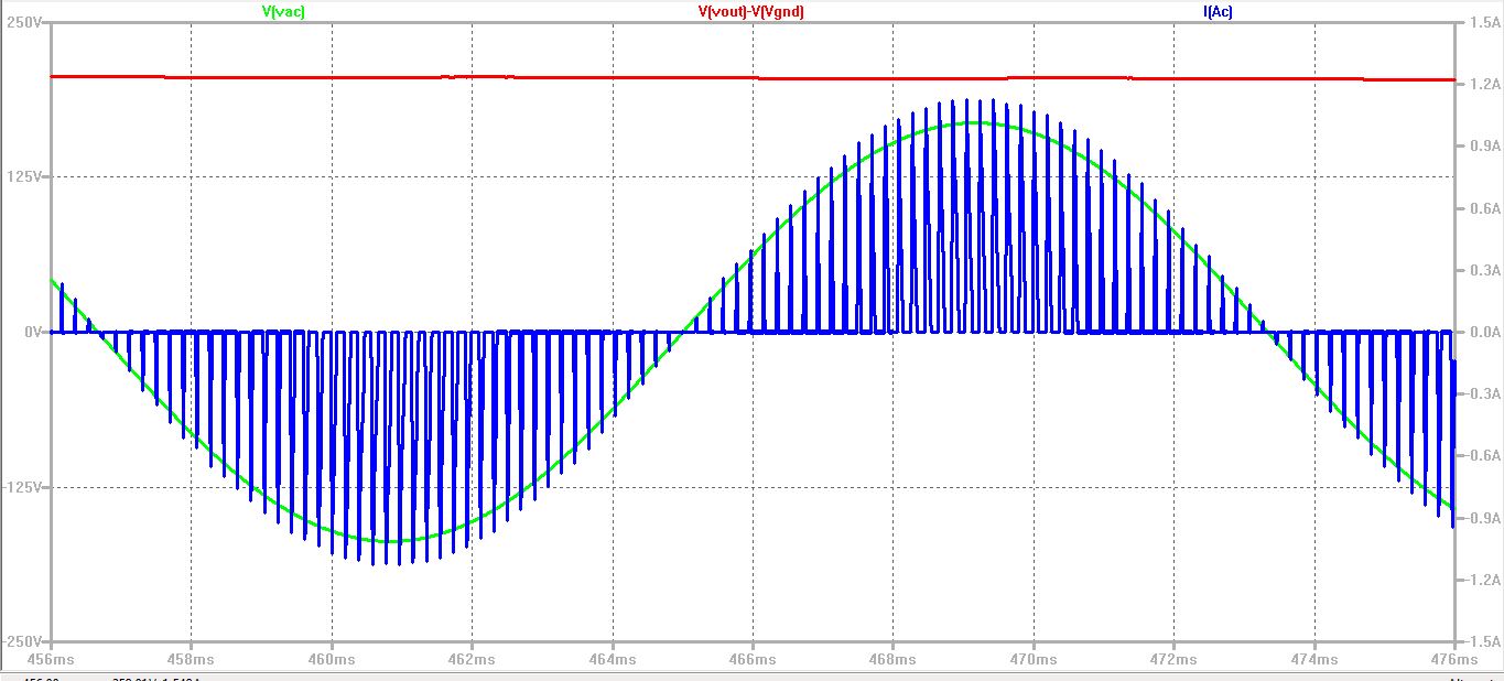
An exaggerated current waveform for a constant on-time boost converter is shown in Figure 9. The AC supply voltage is shown as V(vac), the unfiltered supply current is shown as I(Ac), and the voltage on the output capacitor is shown as V(vout). Notice that the average of the current waveform into the boost converter approximates sinusoidal and is in phase with the voltage. The switching speed shown here is very slow to make the individual pulses more visible. Speeding up the switching would make filtering the switch noise simpler, and operating in continuous conduction mode would further reduce the amplitude of the individual switch cycles.
Another advantage to the boost topology is that the actual switching supply — behind the power factor correcting front end — now operates from a relatively fixed voltage. If the boost stage can accommodate a wide input range, the requirement for the rest of the supply to meet this input is mitigated.
Other topologies exist, each with their own sets of advantages and disadvantages. Some power supply modules are available now with the power factor correction built in; they just require an input capacitor, a boost capacitor, and an output capacitor. Whatever solution is chosen, simulating the design is highly recommended, because it will provide greater insight into how the circuit responds to the corner cases. TI’s Tina, Intersil’s online simulator, and Linear Technologies’ LTspice are among the choices available for simulation. With many solutions available, power factor correction is not as daunting a task as it once was.
About The Author
Jeff Prsha is a design engineer for A2e Technologies, a design services firm in San Diego, CA. Jeff has a degree in electrical engineering from UCLA and has been generating thoughtful solutions to medical, avionic, marine, and industrial applications for 35 years. He is a hands-on engineer and an inventor on 17 patents.