
Silicon: A Material With Huge Potential For Lab-On-Chips
By Paolo Fiorini, principal scientist, imec
Lab-on-chips (LOCs) promise a revolution in healthcare, bringing diagnostics closer to doctors and patients, and giving researchers and drug discoverers faster tools. Across the world, research groups are looking for the best ways to develop compact and reliable LOC systems. The nano-electronics research center imec and its partners are also on this quest. One of their developments is a silicon-based platform for microfluidic structures with great design flexibility. While polymers will remain the best choice for less-demanding LOC systems, silicon is the way to go if you want to shrink dimensions of microfluidics components and combine electrical functionality and sensing in the same chip.
Today, if you want to have your blood analyzed, you go to see your doctor and he or she sends the sample to a specialized lab. After a few days, you receive the results and can take action if needed. Experts from the healthcare and electronics sector believe that this work flow will change when lab-on-chips (LOCs) become widely used.
Initially, LOC systems will be available at doctors’ offices or in hospitals (so-called points of care) as desktop tools, into which a cartridge with a blood droplet must be inserted. The cartridge is disposable and houses the microfluidics and sensors. In the desktop tool, external pumps and heating elements move the fluids in the cartridge and allow the chemical reactions to run at the right temperature.
But eventually, it will be possible to shrink this whole system (with pumps and heating elements) into a few cubic centimeters (see Figure 1). And according to imec, the secret lies in the use of silicon as base material, even for the microfluidics part of the LOC.

Figure 1: Imec envisions lab-on-chip (LOC) devices that are so compact that they can be used at the “point of need.” No desktop tools will be required to read the measurements of the LOC — a simple smartphone will be sufficient to act as user interface.
Polymers, Glass, And Silicon To Make The Blood Flow
An LOC is a device in which a sample (e.g., blood) moves through miniature channels to integrated mixers, reaction chambers, detectors, etc. All these components have one common goal: to detect a target in the sample. This can be proteins, metabolites, ions, or even DNA and RNA. Different materials (polymers, glass, and silicon, or combinations of these) can be used to make these miniaturized integrated structures, and several techniques can be used to circulate the fluid in the device (pressure, capillary, centrifugal, electrokinetic, acoustic, etc.).
The most widespread materials to make these channels and components are polymers. Polymers can be injected in a mold to form the required structures. Another technique is to use photosensitive polymers and lithography to work out the microfluidics. Lithography has the advantage that it is compatible with silicon processing and allows silicon components (e.g., detectors or actuators) to be combined with polymer fluidics (see Figure 2).
Glass and silicon can also be used to make the microfluidic structures. In the latter case, a silicon wafer is patterned (using lithography and dry etch, for example), and the structures are sealed with glass. At the back of the wafer, fluidic connections are carved out to connect the system to the reagent reservoirs and outlets.
Silicon-based microfluidics is considered an expensive option, especially when making a simple passive microfluidic chip with just a few simple components, like microchannels and a mixer. However, the strength of silicon surfaces when making LOCs with a myriad of very fine channels, reaction chambers, and sensors. When integration and sensing are the key assets of the system, then silicon is definitely the best option.
Parallelization is another huge plus of using silicon. Silicon technology (developed by the semiconductor industry) is extremely good at making hundreds of structures in a cost-effective way. So, for LOC applications in which compactness, with ultrafine and numerous structures, is important, silicon definitely is the winner.
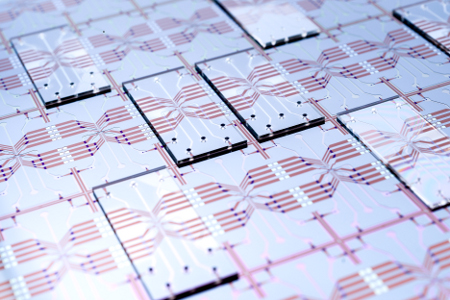
Figure 2: Microfluidic structures made at imec. The structures are made in polymers on a silicon wafer and sealed with glass plates.
A Silicon-Based Platform For Microfluidics
To prove the potential of silicon for microfluidics, imec developed a process flow building on its semiconductor fabrication expertise. Both coarse (500 to 3 µm) and fine (3 to 0.5 µm) structures can be made within the same process flow, which is not obvious when using deep silicon etch techniques. This results in great design flexibility. Also, structures with high aspect ratios can be fabricated (up to aspect ratio 40). A good example of this is the high, narrow micropillars that were made for use as, e.g., filters. The process flow is discussed in more detail in Figure 3.
A variety of structures was made using this process flow: microchannels, mixers, microreactors, micropillar filters, capillary pumps and valves, droplet generators (for digital droplet polymerase chain reaction, or dPCR), mergers, and splitters (see Figure 4). The process has proved to be very stable and can be used for a variety of designs.

Figure 3: Process flow to make both fine and coarse microfluidic structures on a silicon wafer. (a) A silicon wafer (grey color) is covered with an oxide layer (green color). The fine structures are patterned in the oxide layer, which will be used as a mask for their fabrication in a later phase. (b) Then, a nitride layer (blue color) is added. (c) An etch is performed to remove nitride and oxide, and silicon is excavated to form the coarse structures. (d) The exposed silicon surface is oxidized. This oxide will serve as protection during the definition of fine structures. (e) The nitride is removed and the fine structures are etched, (f) the oxide is removed, and (g) the silicon is bonded to Pyrex. (h) A backside etch is performed to open fluidic connections. Note that thanks to the fact that an oxide mask with nitride protection is used, it is not necessary to spin and pattern the resist for fine structure etching, which would be difficult due to the large topography of the already defined coarse structures.
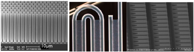
Figure 4: SEM pictures of some of the structures that were made with imec’s silicon-based microfluidic platform: (1) micropillar filter for DNA separation in high performance liquid chromatography tools, (2) crossflow filter for removing cell debris in lysed blood, and (3) array of specially shaped pillars forming an evenly filling capillary pump.
A Lab-On-Chip For SNP Detection
Imec, together with one of its partners (Panasonic), used this silicon-based microfluidics platform to make an LOC for the detection of single nucleotide polymorphisms (SNPs). These are variations in DNA of only one base-pair that are important to predict, for example, the response of an individual patient to a certain drug.
For example, these mutations can predict if breast cancer patients will benefit from tamoxifen, or if colon cancer patients will benefit from cetuximab. And sometimes, the situation is more complex because multiple SNPs determine the response to a specific drug. Determining these SNPs is important when moving to personalized medicine, where patients receive drugs not only based on their disease but also on their personal profile (DNA, RNA, proteins, etc.).
The LOC for SNP detection consists of three major parts (see Figure 5): the silicon chip with microfluidics, a plastic layer with pumps, valves and detector, and a PCB to connect the electrical connections of the pump, valves, and detector to the benchtop machine.
Let’s focus on the microfluidic silicon chip and follow the way the blood sample flows in the chip. First, the blood sample is loaded. Second, the pumps push the blood and reagents towards the pre-amplification module. This module consists of a mixer, a thermal reactor for PCR, and a filter. With these components, the following steps are performed: the white blood cells are lysed, DNA is released, DNA is amplified, and lysate passes through a filter that retains the debris of cells while the DNA is able to pass to the next module. Third, in the analysis module, the purified DNA is mixed with reagents, allele-specific PCR is performed so that only the DNA fragments with the SNP are amplified, and byproducts of the amplification are detected with an electrochemical detector.
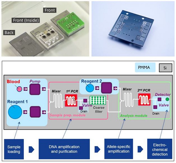
Figure 5: PCR chip made by imec and Panasonic, based on a silicon-based microfluidic platform. (a) Silicon chip for the detection of a single SNP. The chip is mounted together with the plastic layer containing pumps and valves, and this again is mounted on a PCB. (b) Silicon chip for multiple SNP detection. (c) Scheme of the structures in the LOC device.
Future Work: From Point-Of-Care To Point-Of-Need Devices
The above LOC that was developed by imec and Panasonic is a fast and reliable tool to detect SNPs, but it still is a desktop tool. If we want such tests to become more widespread (e.g., also in remote areas or developing countries), the tools have to become even smaller and cheaper. To be able to shrink the desktop tool into a few square centimeters, pumps, valves, and cooling/heating systems need be drastically miniaturized.
Imec researchers are therefore developing capillary pumps and valves to move the fluid through the LOC without the need for external pumps and valves. Also, they are introducing a backside metal layer into the platform as described in Figure 3 to make thin-film heaters and temperature sensors and eliminate the external cooling and heating systems. Another adaptation to the platform will be to work out a low-temperature bonding (preferably room temperature), which can replace the current anodic bonding that is performed at 400° C. This will allow us to functionalize the chip within one and the same process flow.